| CPC H01L 27/156 (2013.01) [H01L 33/0075 (2013.01); H01L 33/0093 (2020.05); H01L 33/06 (2013.01); H01L 33/58 (2013.01); H01L 33/32 (2013.01); H01L 33/42 (2013.01)] | 9 Claims |

|
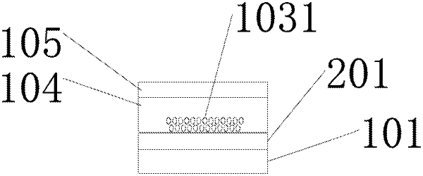
1. A light emitting diode, comprising:
a first-type layer, which comprises a first-type gallium nitride;
a light emitting layer, which is located on the first-type layer and comprises a quantum dot;
a second-type layer, which is located on the light emitting layer and comprises an indium tin oxide (ITO);
an electrode layer, which is located on the second-type layer;
a black matrix, which is located between the first-type layer and the second-type layer and comprises a first window, and the light emitting layer is located within the first window; and
an insulating layer, which covers an upper surface of the electrode layer, a side surface of the electrode layer, and a side surface of the second-type layer.
|