| CPC H01L 27/14629 (2013.01) [H01L 27/14621 (2013.01); H01L 27/1463 (2013.01); H01L 27/14645 (2013.01); H01L 27/14685 (2013.01)] | 20 Claims |

|
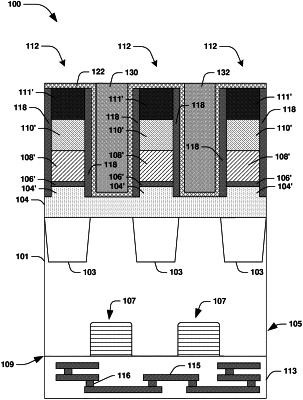
1. A method of forming a semiconductor device, comprising:
forming a metal structure over a first dielectric layer and overlying a portion of a substrate between a first pixel and a second pixel;
forming a first barrier layer over the metal structure and the first dielectric layer;
removing a first portion of the first barrier layer over the first dielectric layer to expose a top surface of the first dielectric layer;
forming a passivation layer over the top surface of the first dielectric layer after removing the first portion of the first barrier layer; and
forming a color filter over the top surface of the first dielectric layer after forming the passivation layer such that a second portion of the first barrier layer is laterally between the color filter and the metal structure.
|