| CPC H01L 27/1461 (2013.01) [H01L 27/14623 (2013.01); H01L 27/14643 (2013.01); H01L 31/107 (2013.01)] | 10 Claims |

|
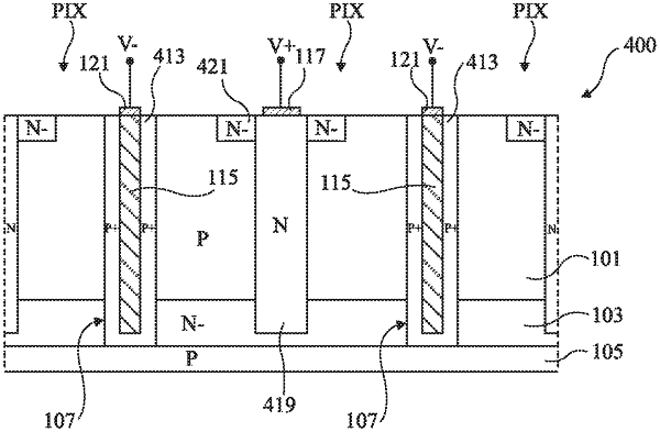
1. An image sensor comprising a plurality of avalanche photodiodes with a vertical PN junction formed inside and on top of a semiconductor substrate of a first conductivity type having a front side and a back side, wherein:
trenches vertically extend in the substrate from its front side to its back side, the trenches having, in top view, the shape of a continuous grid laterally delimiting a plurality of substrate islands, each island defining a pixel comprising a single individually-controllable avalanche photodiode with a vertical PN junction, and comprising a doped area of collection of an avalanche signal of the pixel photodiode;
the lateral walls of the trenches are coated with a first semiconductor layer having a conductivity type opposite to that of the collection area; and
a conductive region extends in the trenches, said conductive region being in contact with the surface of the first semiconductor layer opposite to the substrate,
the sensor further comprising, in a central portion of each substrate island, a central region having a conductivity type opposite to that of the substrate forming the collection area of the island, vertically extending in the substrate from its front side to its back side, the junction between the lateral surfaces of the central region having a conductivity type opposite to that of the substrate and the substrate defining an avalanche area of an avalanche photodiode of the sensor.
|