| CPC H01L 27/1461 (2013.01) [H01L 25/167 (2013.01); H01L 27/14643 (2013.01); H01L 31/0224 (2013.01); H04N 25/705 (2023.01); H04N 25/75 (2023.01); H04N 25/778 (2023.01)] | 20 Claims |

|
1. A uniform-bridge-gradient (UBG) time-of-flight (ToF) photodiode block comprising:
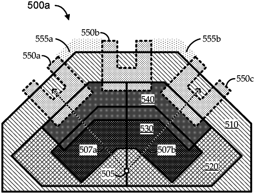
a plurality of taps disposed onto a semiconductor substrate of a first doping type, the plurality of taps comprising at least a first readout tap and a second readout tap, each of the plurality of taps having one of a plurality of transfer gates configured for selective activation by an activation network;
a photodiode region implanted into the semiconductor substrate and comprising:
a photodiode-defining implant of a second doping type complementary to the first doping type implanted to a first implant depth over the photodiode region;
a first bridging implant of the second doping type implanted to a second implant depth over a first portion of the photodiode region that forms a first lateral bridge region across the plurality of taps along an edge of the photodiode region nearest to the plurality of taps; and
a second bridging implant of the second doping type implanted to a third implant depth over a second portion of the photodiode region that forms a second lateral bridge region across the plurality of taps and at least partially overlaps with both the photodiode-defining implant and the first bridging implant, the third implant depth being deeper than both the first implant depth and the second implant depth.
|