| CPC H01L 27/14605 (2013.01) [B60R 1/001 (2013.01); G02B 23/2407 (2013.01); H01L 27/14621 (2013.01); H04N 25/766 (2023.01); H04N 23/555 (2023.01)] | 6 Claims |

|
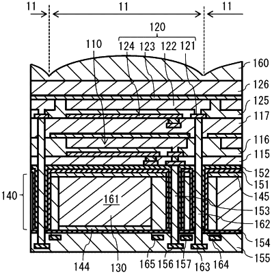
1. A solid-state imaging device, comprising:
a plurality of pixels;
a plurality of stacked photoelectric converters, wherein one stacked photoelectric converter of the plurality of stacked photoelectric converters is included in each pixel of the plurality of pixels, each of the stacked photoelectric converters having a plurality of photoelectric conversion elements stacked therein, the plurality of photoelectric conversion elements each having different wavelength selectivity; and
a plurality of data output lines from which pixel signals are outputted, the pixel signals being based on electric charges outputted from the photoelectric conversion elements,
wherein a number of the data output lines is provided for each of a plurality of predetermined unit pixel columns,
wherein the number of the data output lines provided for each of the plurality of predetermined unit pixel columns is equal to an integer multiple of the photoelectric conversion elements stacked in each of the stacked photoelectric converter,
wherein a first stacked photoelectric converter of the plurality of photoelectric converters includes a first photoelectric conversion element, a second photoelectric conversion element, and a first color filter provided between the first photoelectric conversion element and the second photoelectric conversion element,
wherein a second stacked photoelectric converter of the plurality of photoelectric converters includes a third photoelectric conversion element, a fourth photoelectric conversion element, and a second color filter provided between the third photoelectric conversion element and the fourth photoelectric conversion element,
wherein the first photoelectric conversion element and the third photoelectric conversion element are configured to selectively perform photoelectric conversion of light of a first color,
wherein the second photoelectric conversion element is configured to perform photoelectric conversion of light of a second color that has transmitted through the first photoelectric conversion element and the first color filter,
wherein the fourth photoelectric conversion element is configured to perform photoelectric conversion of light of a third color that has transmitted through the third photoelectric conversion element and the second color filter,
wherein a first data output line is provided for the first photoelectric conversion element and the third photoelectric conversion element, and
wherein a second data output line is provided for the second photoelectric conversion element and the fourth photoelectric conversion element.
|