| CPC H01L 27/124 (2013.01) [G02F 1/136227 (2013.01); G02F 1/136286 (2013.01); G02F 1/1368 (2013.01); G09G 3/3225 (2013.01); G09G 3/3266 (2013.01); H01L 27/1259 (2013.01); H10K 59/123 (2023.02); H10K 59/124 (2023.02); H10K 59/131 (2023.02); G02F 1/136295 (2021.01); G09G 2300/0861 (2013.01); H01L 27/1225 (2013.01); H01L 27/1255 (2013.01); H10K 59/1201 (2023.02)] | 5 Claims |

|
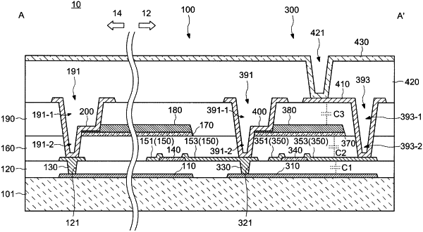
1. A semiconductor device comprising:
a first gate electrode;
a first gate insulating layer above the first gate electrode;
a first oxide semiconductor layer above the first gate insulating layer;
a source electrode and a drain electrode connected to the first oxide semiconductor layer;
a second gate insulating layer above the first oxide semiconductor layer;
a second gate electrode above the second gate insulating layer;
a first insulating layer above the second gate electrode;
a second oxide semiconductor layer between the second gate insulating layer and the second gate electrode;
a first aperture penetrating the first insulating layer and the second gate insulating layer, a part of the first aperture overlapping the second oxide semiconductor layer in a planar view;
a first connecting electrode in the first aperture;
a second aperture penetrating the first gate insulating layer; and
a second connecting electrode in the second aperture,
wherein
the first connecting electrode is connected to the second gate electrode and the second connecting electrode, and
the second connecting electrode is connected to the first gate electrode.
|