| CPC H01L 25/165 (2013.01) [H01L 21/561 (2013.01); H01L 21/565 (2013.01); H01L 23/3121 (2013.01); H01R 13/665 (2013.01); H01L 23/24 (2013.01); H01L 23/49811 (2013.01); H01L 24/32 (2013.01); H01L 24/33 (2013.01); H01L 24/48 (2013.01); H01L 24/73 (2013.01); H01L 2224/32145 (2013.01); H01L 2224/32225 (2013.01); H01L 2224/33181 (2013.01); H01L 2224/48145 (2013.01); H01L 2224/48227 (2013.01); H01L 2224/73215 (2013.01); H01L 2224/73265 (2013.01); H01R 24/62 (2013.01)] | 20 Claims |

|
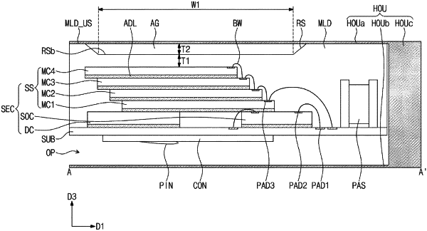
1. A semiconductor package, comprising:
a package substrate;
a semiconductor chip on the package substrate, the semiconductor chip including a logic chip and a memory stack structure on the logic chip;
a connector and a connector terminal below the package substrate;
a molding layer that covers the semiconductor chip, the molding layer having a recess region on a top surface of the molding layer;
a housing that covers the molding layer; and
an air gap on the semiconductor chip, the air gap being defined by the housing and the recess region of the molding layer, and the molding layer separating the air gap from the memory stack structure of the semiconductor chip,
wherein a portion of the molding layer is disposed between a top surface of the semiconductor chip and a bottom surface of the recess region.
|