| CPC H01L 25/0753 (2013.01) [H01L 25/167 (2013.01); H01L 33/0095 (2013.01); H01L 33/385 (2013.01); H01L 33/44 (2013.01); H01L 33/60 (2013.01); H01L 33/0093 (2020.05); H01L 33/405 (2013.01); H01L 2933/0016 (2013.01); H01L 2933/0025 (2013.01); H01L 2933/0058 (2013.01)] | 16 Claims |

|
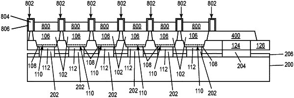
1. An optical projection device, comprising:
a plurality of LEDs (light-emitting diodes), the LEDs each comprising a semiconductor mesa laterally spaced apart from one another by a grid structure,
wherein each of the semiconductor mesas comprises an n-type material and a p-type material adjoining at least partly the n-type material,
wherein the grid structure at least partly laterally surrounds at least the n-type material of each of the semiconductor mesas,
wherein the grid structure comprises a conductive material that electrically interconnects the n-type material of the semiconductor mesas,
wherein the grid structure is configured to block optical crosstalk between light emitted by the LEDs,
wherein the semiconductor mesas are coplanar with an upper surface of the grid structure,
wherein the optical projection device further comprises:
a separate light conversion layer arranged on at least some of the semiconductor mesas and configured to convert a wavelength of light emitted by the semiconductor mesa aligned with the respective separate light conversion layer; and
an isolation structure laterally surrounding each of the separate light conversion layers and configured to block optical crosstalk between the separate light conversion layers,
wherein the isolation structure comprises:
a wall made of an electrically insulating material and configured to block optical crosstalk between the separate light conversion layers; and
a metal or metal alloy coating the electrically insulating material.
|