| CPC H01L 25/0657 (2013.01) [H01L 21/4853 (2013.01); H01L 21/486 (2013.01); H01L 21/565 (2013.01); H01L 23/13 (2013.01); H01L 23/3164 (2013.01); H01L 23/5384 (2013.01); H01L 23/5386 (2013.01); H01L 25/18 (2013.01); H01L 25/50 (2013.01); H01L 2225/06517 (2013.01); H01L 2225/06548 (2013.01); H01L 2225/06558 (2013.01)] | 20 Claims |
|
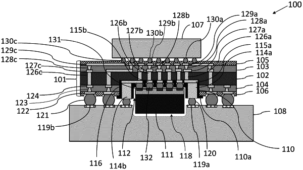
1. A semiconductor package comprising:
a substrate with a top surface and a bottom surface;
a substrate recess in the bottom surface of the substrate;
a first device positioned over the top surface of the substrate, wherein the first device at least partially overlaps the substrate recess;
a mold material in the substrate recess, the mold material overlapping the bottom surface of the substrate adjacent to the substrate recess;
a second device positioned in the substrate recess; and
a plurality of interconnect vias in the substrate, wherein at least one of the plurality of interconnect vias is coupled to the first and second devices to provide an electrical connection therebetween.
|