| CPC H01L 23/552 (2013.01) [H01L 21/56 (2013.01); H01L 23/3107 (2013.01); H01L 23/4952 (2013.01); H01L 24/48 (2013.01); H01L 24/85 (2013.01); H01L 2224/48245 (2013.01); H01L 2224/85035 (2013.01); H01L 2224/85203 (2013.01); H01L 2224/85205 (2013.01)] | 20 Claims |

|
1. A package structure, comprising:
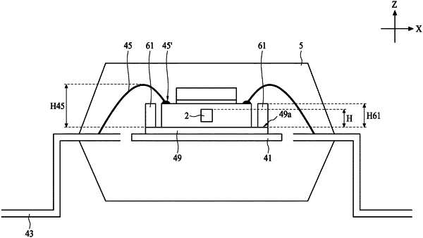
a mounting pad having a mounting surface;
a semiconductor chip having a magnetic device,
wherein the semiconductor chip comprises:
a first surface perpendicular to a thickness direction of the semiconductor chip;
a second surface opposite to the first surface, wherein the second surface is attached to the mounting surface of the mounting pad; and
a third surface connecting the first surface and the second surface;
a first magnetic field shielding including a plurality of segments laterally at least partially surrounding the semiconductor chip and facing the third surface of the semiconductor chip, wherein a bottom surface of the first magnetic field shielding is attached to the mounting surface of the mounting pad, wherein the mounting surface comprises first portion free from overlapping with the first magnetic field shielding from a top view perspective; and
a bonding wire electrically connecting the first surface and a lead frame,
wherein at least one segment of the first magnetic field shielding is disposed between the bonding wire and the third surface of the semiconductor chip.
|