| CPC H01L 23/544 (2013.01) [G03F 9/708 (2013.01); H01L 21/76802 (2013.01); H01L 23/5226 (2013.01); H01L 2223/54426 (2013.01)] | 12 Claims |

|
1. A semiconductor device, comprising:
a substrate;
a dielectric stack positioned on the substrate;
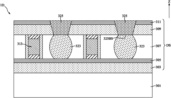
two second conductive features positioned in the dielectric stack;
a decoupling unit positioned in the dielectric stack, between the two second conductive features, wherein the decoupling unit has low dielectric constant for providing decoupling function and for reducing parasitic capacitance of the second conductive features; and
an alignment mark positioned on the decoupling unit;
wherein the alignment mark comprises a fluorescent material; wherein the fluorescent material comprises azobenzene; wherein the decoupling unit comprises a porous low-k material;
wherein the dielectric stack comprises a first dielectric layer positioned on the substrate, a second dielectric layer positioned on the first dielectric layer, a middle dielectric layer positioned on the second dielectric layer, a third dielectric layer positioned on the middle dielectric layer, and a fourth dielectric layer positioned on the third dielectric layer, and the two second conductive features and the decoupling unit are positioned in the middle dielectric layer.
|