| CPC H01L 23/4985 (2013.01) [H01L 23/49838 (2013.01); H01L 23/49894 (2013.01); H01L 24/73 (2013.01); H01L 2224/73204 (2013.01)] | 20 Claims |

|
1. A chip-on-film package, comprising:
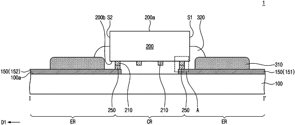
a film substrate including a chip region and an edge region;
a plurality of lead lines on a top surface of the edge region of the film substrate, the lead lines comprising first and second lead lines;
a semiconductor chip on a top surface of the chip region of the film substrate, the semiconductor chip comprising a row of chip pads, the row of chip pads including at least a first chip pad and a second chip pad, and at least two third chip pads spaced apart from each other in a first horizontal direction such that the first chip pad and the second chip pad are between the third chip pads in the first horizontal direction and such that the row of chip pads is spaced apart from the third chip pads in a second horizontal direction;
a plurality of redistribution patterns on a bottom surface of the semiconductor chip, the plurality of redistribution patterns comprising first, second and third redistribution patterns;
a first connection terminal connecting the first redistribution pattern and the first lead line; and
a second connection terminal connecting the second redistribution pattern and the second lead line,
wherein the first chip pad, the first redistribution pattern and the first connection terminal are vertically aligned,
the second redistribution pattern extends horizontally from a bottom surface of the second chip pad, and only a portion of the second redistribution pattern vertically overlaps with the second connection terminal,
the third redistribution pattern connects the third chip pads across the semiconductor chip, when viewed in a plan view, and
wherein the first horizontal direction and the second horizontal direction are different from each other.
|