| CPC H01L 23/4985 (2013.01) [H01L 23/49822 (2013.01); H01L 23/49833 (2013.01); H01L 24/16 (2013.01); H01L 24/32 (2013.01); H01L 24/73 (2013.01); H01L 25/072 (2013.01); H01L 2224/16225 (2013.01); H01L 2224/32225 (2013.01); H01L 2224/73253 (2013.01); H01L 2924/182 (2013.01); H01L 2924/30107 (2013.01)] | 14 Claims |

|
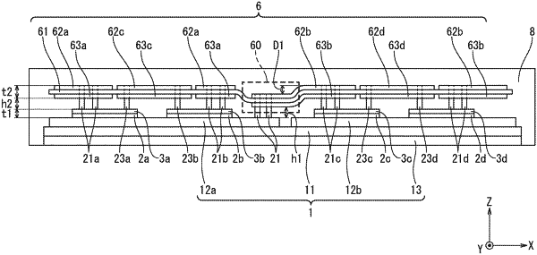
1. A semiconductor device comprising:
an insulated circuit substrate including first and second conductive layers on a top surface side;
a first semiconductor chip mounted on the first conductive layer;
a second semiconductor chip mounted on the second conductive layer;
a printed circuit board including an insulating layer, a first lower-side wiring layer arranged on one main surface of the insulating layer so as to be opposed to the first semiconductor chip, and a second lower-side wiring layer arranged on the one main surface of the insulating layer so as to be opposed to the second semiconductor chip, the printed circuit board being provided with a curved part curved toward the insulated circuit substrate;
a first connection member arranged to connect the first semiconductor chip with the first lower-side wiring layer;
a second connection member arranged to connect the second semiconductor chip with the second lower-side wiring layer;
a third connection member arranged to connect the first conductive layer with the second lower-side wiring layer at the curved part; and
a sealing member provided to seal the first and second semiconductor chips, the printed circuit board, and the first to third connection members.
|