| CPC H01L 23/49838 (2013.01) [H01L 21/4846 (2013.01); H01L 23/66 (2013.01); H01L 23/49827 (2013.01); H01L 23/50 (2013.01); H01L 23/5383 (2013.01); H01L 25/16 (2013.01); H01L 2223/6666 (2013.01)] | 20 Claims |

|
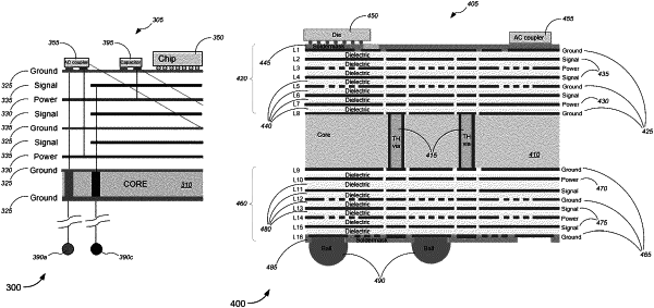
1. A semiconductor package, comprising:
a semiconductor substrate comprising:
a core layer;
a first plurality of layers disposed on or above the core layer, the first plurality of layers comprising:
one or more first power layers disposed on or above the core layer;
one or more first ground layers disposed on or above the core layer;
one or more first signal layers disposed on or above the core layer, each signal layer among the one or more first signal layers being disposed between a closest power layer among the one or more first power layers and a closest ground layer among the one or more first ground layers, the closest power layer and the closest ground layer each providing a return path for high frequency signals carried by said each signal layer; and
a plurality of first dielectric layers, each dielectric layer being disposed between and in contact with two of a power layer among the one or more first power layers, a ground layer among the one or more first ground layers, or a signal layer among the one or more first signal layers; and
at least one alternating current (“AC”) coupler coupled to each of at least one power layer among the one or more first power layers and at least one ground layer among the one or more first ground layers, without any portion of any of the one or more first power layers that is within a first distance from an edge of the core layer being anchored to the core layer, the first distance being half a distance between the edge of the core layer and a closest edge of one of a semiconductor chip or a mount for the chip that is mounted on or above the semiconductor substrate.
|