| CPC H01L 23/49833 (2013.01) [H01L 23/49822 (2013.01); H01L 23/49838 (2013.01); H01L 23/49894 (2013.01); H01L 23/645 (2013.01); H01L 24/16 (2013.01); H01L 2224/16225 (2013.01); H01L 2924/19042 (2013.01); H01L 2924/19103 (2013.01)] | 24 Claims |
|
1. A package substrate, comprising:
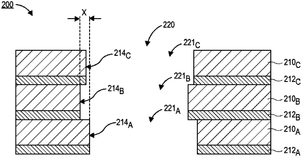
a plurality of glass layers, wherein one of the plurality of glass layers has a vertical sidewall that is recessed relative to a corresponding vertical sidewall of an overlying one of the plurality of glass layers and relative to a corresponding vertical sidewall of an underlying one of the plurality of glass layers;
a plurality of dielectric layers, wherein the glass layers alternate with the dielectric layers, and wherein each of the plurality of glass layers has a thickness greater than a thickness of each one of the plurality of dielectric layers;
a through-hole through the plurality of glass layers and the plurality of dielectric layers; and
a conductive through-hole via in the through-hole.
|