| CPC H01L 23/4093 (2013.01) [H01L 23/4006 (2013.01); H01L 2023/405 (2013.01); H01L 2023/4087 (2013.01); H01L 24/48 (2013.01); H01L 2224/48245 (2013.01)] | 20 Claims |

|
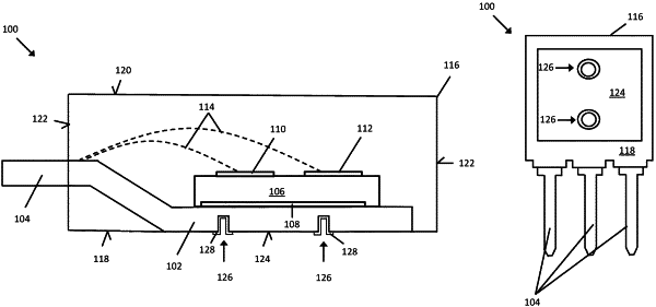
1. A semiconductor package, comprising:
a lead frame that comprises a die pad and a plurality of leads;
a semiconductor die mounted on a die attach surface of the die pad;
an encapsulant body of electrically insulating material that covers semiconductor die and portions of the lead frame; and
a fastener receptacle that comprises a blind hole in the encapsulant body or the die pad, and
wherein a rear surface of the die pad is exposed from a first main face of the encapsulant body.
|
|
13. A semiconductor assembly comprising:
a heat sink;
a semiconductor package comprising an encapsulant body of electrically insulating material, a die pad with a rear surface that is exposed from a first main face of the encapsulant body, and a fastener receptacle that comprises a blind hole in the encapsulant body or the die pad; and
a fastener that is securely retained by the fastener receptacle and affixes the semiconductor package to the heat sink.
|