| CPC H01L 23/3178 (2013.01) [H01L 23/3192 (2013.01); H01L 23/49822 (2013.01); H01L 23/49861 (2013.01)] | 20 Claims |
|
1. A device comprising:
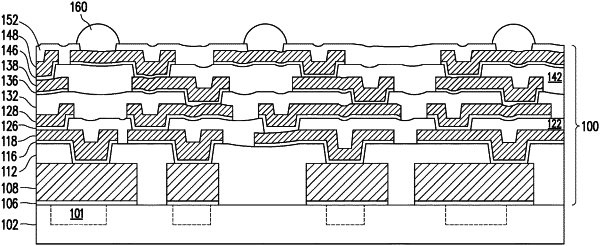
a redistribution structure coupled to a conductive feature of a substrate, the redistribution structure comprising:
a first conductive layer,
a first insulating layer over the first conductive layer, the first insulating layer comprising a first filler-free insulating material,
a second conductive layer over the first insulating layer, the second conductive layer coupled to the first conducting layer, and
a second insulating layer over the second conductive layer, the second insulating layer comprising a second filler-free insulating material, wherein an upper surface of the second insulating layer is wavy, wherein a difference between an average peak of the upper surface and an average valley of the upper surface is between 3 μm and 5 μm; and
a conductive connector electrically coupled to the redistribution structure.
|