| CPC H01L 23/3128 (2013.01) [H01L 23/5383 (2013.01); H01L 24/16 (2013.01); H01L 24/32 (2013.01); H01L 25/0652 (2013.01); H01L 2224/16227 (2013.01); H01L 2224/32145 (2013.01); H01L 2225/06548 (2013.01)] | 20 Claims |

|
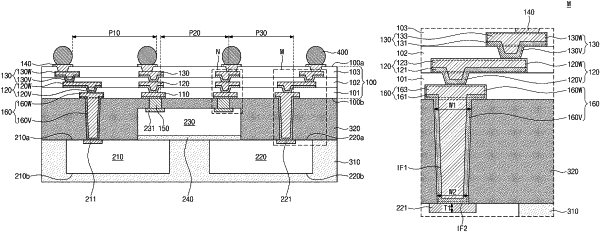
1. A semiconductor package, comprising:
a redistribution substrate comprising a first surface and a second surface, which are opposite each other;
a first semiconductor chip on the first surface of the redistribution substrate;
a first molding portion on a side surface of the first semiconductor chip;
a second semiconductor chip between the first semiconductor chip and the redistribution substrate;
a second molding portion between the redistribution substrate and the first molding portion, the second molding portion on a side surface of the second semiconductor chip;
bump patterns between the second semiconductor chip and the redistribution substrate; and
a mold via penetrating the second molding portion and electrically connecting the first semiconductor chip to the redistribution substrate, wherein
the redistribution substrate comprises an insulating layer, a first redistribution pattern in the insulating layer, and a second redistribution pattern in the insulating layer,
the first redistribution pattern and the second redistribution pattern are sequentially stacked in a direction from the first surface of the redistribution substrate toward the second surface,
the mold via is in contact with the second redistribution pattern, and
the bump patterns are in contact with the first redistribution pattern.
|