| CPC H01L 21/76843 (2013.01) [H01L 21/28568 (2013.01); H01L 21/76802 (2013.01); H01L 21/76876 (2013.01)] | 20 Claims |
|
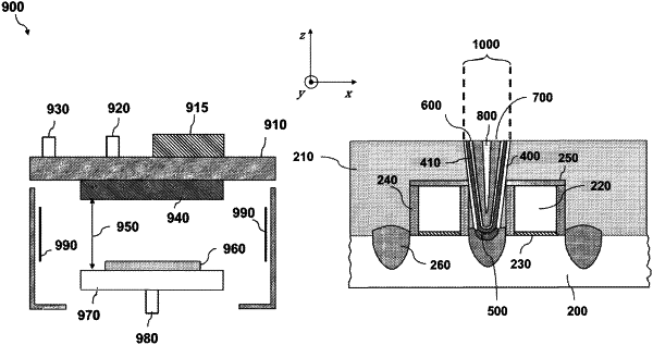
1. A method comprising:
depositing a first metal layer to partially fill an opening in a dielectric layer on a substrate;
depositing a second metal layer on the first metal layer to fill the opening, wherein depositing the second metal layer comprises:
sputter depositing the second metal layer from a metal target by applying a first radio frequency (RF) power to bias the metal target;
reflowing the second metal layer by applying a second RF power to bias the substrate; and
changing the first and second RF powers independently to adjust a ratio of the second RF power to the first RF power while reflowing the second metal layer.
|