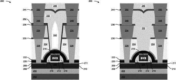
| CPC H01L 21/7682 (2013.01) [H01L 21/28518 (2013.01); H01L 21/76805 (2013.01); H01L 21/76895 (2013.01); H01L 23/5329 (2013.01); H01L 23/535 (2013.01); H01L 29/45 (2013.01); H01L 29/78 (2013.01)] | 20 Claims |

|
1. A semiconductor device, comprising:
a source on a first side of a gate;
a drain on a second side of the gate, the second side of the gate being opposite to the first side of the gate;
a first contact over the source;
a second contact over the drain;
an air gap over the gate between at least the first contact and the second contact;
at least two dielectric materials in each of a region between the air gap and the first contact and a region between the air gap and the second contact; and
a liner layer that is over the first contact and the second contact and that is under the air gap.
|
|
13. A semiconductor device comprising:
a first contact on a first side of a gate;
a second contact on a second side of the gate;
a first dielectric material, between the first contact and the second contact, comprising a first portion adjacent to the first contact and a second portion adjacent to the second contact;
a second dielectric material between the first portion of the first dielectric material and the second portion of the first dielectric material, the second dielectric material being over the gate,
wherein a dielectric constant of the first dielectric material is greater than a dielectric constant of the second dielectric material; and
a liner layer that is over the first contact and the second contact.
|
|
20. A semiconductor device, comprising:
a source and a drain that are each on a gate;
an air gap over the gate between a first contact, over the source, and a second contact over the drain;
a dielectric material in a region between the air gap and the first contact and a region between the air gap and the second contact; and
a liner layer that is over the first contact and the second contact and that is under the air gap.
|