| CPC H01L 21/76808 (2013.01) [H01L 21/0206 (2013.01); H01L 21/0337 (2013.01); H01L 21/0332 (2013.01); H01L 21/76829 (2013.01); H01L 23/5226 (2013.01); H01L 23/53228 (2013.01)] | 20 Claims |
|
1. A method for fabricating a semiconductor device, comprising:
providing a substrate;
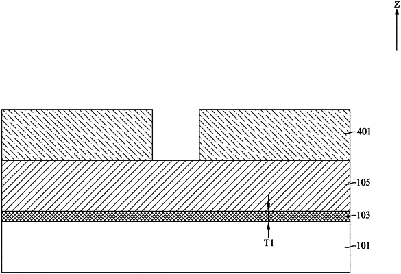
forming a dielectric layer on the substrate;
forming a via opening in the dielectric layer using a first mask layer as a mask;
forming a failed hard mask layer to fill the via opening;
forming a second mask layer on the failed hard mask layer;
removing the second mask layer and the failed hard mask layer;
forming an underfill layer to fill the via opening;
forming a top hard mask layer on the underfill layer;
forming a third mask layer on the top hard mask layer;
patterning the top hard mask layer using the third mask layer as a mask;
forming a trench opening in the dielectric layer using the top hard mask layer as a mask; and
forming a via in the via opening and forming a trench in the trench opening.
|