| CPC H01L 21/486 (2013.01) [H01L 21/481 (2013.01); H01L 22/20 (2013.01); H01L 22/32 (2013.01); H01L 23/481 (2013.01); H01L 23/49827 (2013.01); H01L 25/0657 (2013.01); H01L 24/13 (2013.01); H01L 24/16 (2013.01); H01L 24/81 (2013.01); H01L 2224/0401 (2013.01); H01L 2224/0557 (2013.01); H01L 2224/13147 (2013.01); H01L 2224/16145 (2013.01); H01L 2224/16146 (2013.01); H01L 2224/16147 (2013.01); H01L 2224/16238 (2013.01); H01L 2224/32145 (2013.01); H01L 2224/48227 (2013.01); H01L 2224/73265 (2013.01); H01L 2224/81191 (2013.01); H01L 2224/81192 (2013.01); H01L 2225/06513 (2013.01); H01L 2225/06517 (2013.01); H01L 2225/06541 (2013.01); H01L 2225/06548 (2013.01); H01L 2225/06565 (2013.01); H01L 2225/06596 (2013.01); H01L 2924/10253 (2013.01); H01L 2924/1434 (2013.01); H01L 2924/15192 (2013.01); H01L 2924/15312 (2013.01); H01L 2924/157 (2013.01)] | 20 Claims |

|
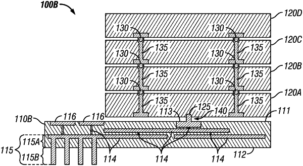
1. A semiconductor device assembly comprising:
a first substrate having a top surface and a bottom surface opposite the top surface;
a second substrate having a top surface and a bottom surface opposite the top surface, the second substrate being disposed over the first substrate;
an interconnect between the first substate and the second substrate that electrically connects the first substrate with the second substrate;
an array of pillars of conductive material that extend outwardly from the bottom surface of the first substrate, the array of pillars being positioned adjacent to a first lateral side of the first substrate and wherein a portion of the array of pillars is positioned within the first substrate;
at least one pad on the top surface of the substrate, the at least one pad being positioned adjacent to the first lateral side of the first substrate;
a plurality of interconnections within the first substrate and coupled at an upper portion of the array of pillars facing the top surface of the substrate, the plurality of interconnections electrically connecting the array of pillars with the interconnect between the first substrate and the second substrate, the at least one pad with the interconnect between the first substrate and the second substrate, and the at least one pad with the array of pillars; and
wherein the first substrate has a first area and the second substrate has a second area that is smaller than the first area and wherein the at least one pad and the array of pillars are offset from the second substrate.
|