| CPC H01L 21/28264 (2013.01) [H01L 21/02164 (2013.01); H01L 21/0228 (2013.01); H01L 29/51 (2013.01); H01L 29/513 (2013.01); H01L 21/02175 (2013.01); H01L 21/02241 (2013.01); H01L 29/2003 (2013.01)] | 5 Claims |
|
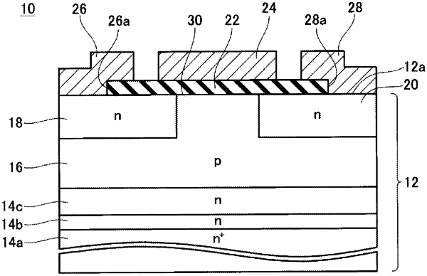
1. A switching device comprising:
a gallium nitride semiconductor layer; and
a gate insulation film made of silicon oxide and disposed above the gallium nitride semiconductor layer,
wherein an interface between the gallium nitride semiconductor layer and the gate insulation film is either free of a gallium oxide layer or provided with the gallium oxide layer with a thickness of 1 nanometer or smaller, and
a dipole is not formed across the interface between the gallium nitride semiconductor layer and the gate insulation film.
|