US 12,191,148 B2
Semiconductor device and manufacturing method thereof
Yasunori Agata, Matsumoto (JP); Takashi Yoshimura, Matsumoto (JP); Hiroshi Takishita, Matsumoto (JP); Misaki Meguro, Matsumoto (JP); Naoko Kodama, Matsumoto (JP); Yoshihiro Ikura, Matsumoto (JP); Seiji Noguchi, Matsumoto (JP); Yuichi Harada, Matsumoto (JP); and Yosuke Sakurai, Azumino (JP)
Assigned to FUJI ELECTRIC CO., LTD., Kanagawa (JP)
Filed by FUJI ELECTRIC CO., LTD., Kanagawa (JP)
Filed on Jul. 20, 2023, as Appl. No. 18/355,426.
Application 18/355,426 is a continuation of application No. 17/748,006, filed on May 18, 2022, granted, now 11,735,424.
Application 17/748,006 is a continuation of application No. 17/033,925, filed on Sep. 28, 2020, granted, now 11,342,186, issued on May 24, 2022.
Application 17/033,925 is a continuation of application No. PCT/JP2019/040241, filed on Oct. 11, 2019.
Claims priority of application No. 2018-196766 (JP), filed on Oct. 18, 2018; application No. 2018-248523 (JP), filed on Dec. 28, 2018; and application No. 2019-159499 (JP), filed on Sep. 2, 2019.
Prior Publication US 2023/0360915 A1, Nov. 9, 2023
Int. Cl. H01L 27/06 (2006.01); H01L 21/22 (2006.01); H01L 21/265 (2006.01); H01L 21/268 (2006.01); H01L 29/06 (2006.01); H01L 29/10 (2006.01); H01L 29/32 (2006.01); H01L 29/40 (2006.01); H01L 29/66 (2006.01); H01L 29/739 (2006.01); H01L 29/861 (2006.01)
CPC H01L 21/221 (2013.01) [H01L 21/26526 (2013.01); H01L 21/268 (2013.01); H01L 27/0664 (2013.01); H01L 29/0623 (2013.01); H01L 29/1095 (2013.01); H01L 29/32 (2013.01); H01L 29/404 (2013.01); H01L 29/66348 (2013.01); H01L 29/7397 (2013.01); H01L 29/8613 (2013.01)] 29 Claims
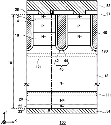
OG exemplary drawing
 
1. A semiconductor device comprising:
a semiconductor substrate having an upper surface and a lower surface, wherein
in a depth direction connecting the upper surface and the lower surface of the semiconductor substrate, a donor concentration distribution includes:
a first donor concentration peak placed at a first depth;
a second donor concentration peak placed at a second depth between the first donor concentration peak and the upper surface, the second donor concentration peak having a lower concentration than the first donor concentration peak;
a flat region placed between the first donor concentration peak and the second donor concentration peak, wherein the donor concentration distribution in the flat region is substantially flat and a thickness of the flat region in the depth direction is 10% or more of a thickness of the semiconductor substrate in the depth direction; and
a plurality of donor concentration peaks placed between the first donor concentration peak and the lower surface.