| CPC H01L 29/742 (2013.01) [H10B 12/10 (2023.02)] | 11 Claims |

|
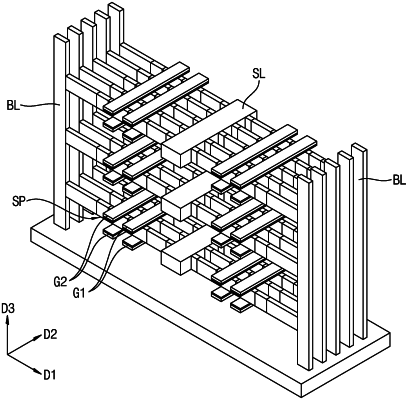
1. A semiconductor device comprising:
a substrate having an upper surface extending in a first horizontal direction and a second horizontal direction crossing the first horizontal direction;
a first conductive line extending longitudinally in the first horizontal direction on the substrate;
a second conductive line spaced apart from the first conductive line in the second horizontal direction and extending longitudinally in a vertical direction on the substrate, the vertical direction is perpendicular to the upper surface of the substrate;
a semiconductor pattern disposed between the first conductive line and the second conductive line, the semiconductor pattern including:
a first semiconductor pattern disposed adjacent to the first conductive line, the first semiconductor pattern having first-conductivity-type impurities;
a second semiconductor pattern disposed adjacent to the second conductive line, the second semiconductor pattern having second-conductivity-type impurities that are different from the first-conductivity-type impurities; and
a third semiconductor pattern disposed between the first semiconductor pattern and the second semiconductor pattern, the third semiconductor pattern including a first region disposed adjacent to the first semiconductor pattern and a second region disposed between the first region and the second semiconductor pattern, wherein at least one of the first region and the second region comprises an intrinsic semiconductor layer, wherein the first to third semiconductor patterns extend longitudinally in the second horizontal direction and are contiguously arranged in the second horizontal direction;
a first gate line crossing the first region and extending in the first horizontal direction; and
a second gate line crossing the second region and extending in the first horizontal direction, wherein the first and second gate lines control a same active device.
|