| CPC H01J 37/32724 (2013.01) [H01L 21/6833 (2013.01); H01J 2237/002 (2013.01); H01J 2237/2007 (2013.01)] | 10 Claims |
|
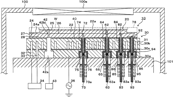
1. A wafer placement table comprising:
a ceramic base having a wafer placement surface in an upper surface and including an electrode;
a cooling base including a coolant flow path formed therein;
a bonding layer bonding a lower surface of the ceramic base and an upper surface of the cooling base;
a stepped hole penetrating the bonding layer and the cooling base in an up-down direction and including an upper hole portion with a small diameter, a lower hole portion with a large diameter, and a hole stepped portion between the upper hole portion and the lower hole portion, the small diameter upper hole portion passing through a region in which the coolant flow path is formed and the large diameter lower hole portion positioned under the coolant flow path;
a stepped insulating pipe inserted through the stepped hole and including an upper pipe portion with a small diameter, a lower pipe portion with a large diameter, and a pipe stepped portion between the upper pipe portion and the lower pipe portion; and
a connection terminal bonded at an upper end to the electrode and inserted through the stepped insulating pipe; and
wherein a diameter of the connection terminal is less than or equal to half of a diameter of the lower pipe portion.
|