| CPC H01J 37/32165 (2013.01) [C23C 16/345 (2013.01); C23C 16/401 (2013.01); C23C 16/4404 (2013.01); C23C 16/45565 (2013.01); H01J 37/32174 (2013.01); H01J 37/32394 (2013.01); H01J 37/32504 (2013.01); H01L 21/02115 (2013.01); H01L 21/02205 (2013.01); H01L 21/02274 (2013.01); H01J 2237/3321 (2013.01)] | 15 Claims |
|
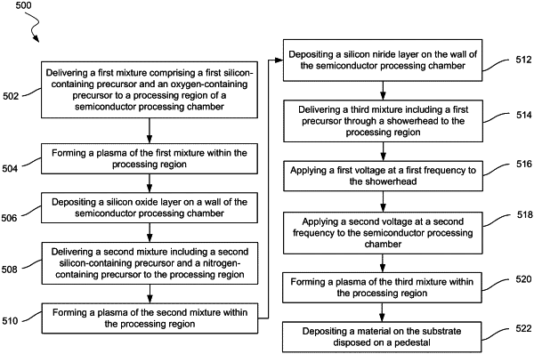
1. A method of depositing material, the method comprising:
delivering a first mixture comprising a first silicon-containing precursor and an oxygen-containing precursor to a processing region of a semiconductor processing chamber;
forming a plasma of the first mixture within the processing region;
depositing a silicon oxide layer on a wall of the semiconductor processing chamber; repeatedly forming alternating layers of silicon oxide and silicon nitride at least five or more times to form a seasoning layer on the wall of the semiconductor processing chamber;
delivering a second mixture comprising a second silicon-containing precursor and a nitrogen-containing precursor to the processing region,
forming a plasma of the second mixture within the processing region;
depositing a silicon nitride layer on the wall of the semiconductor processing chamber;
delivering a third mixture comprising a first precursor through a showerhead to the processing region;
applying a first voltage at a first frequency to the showerhead;
striking a plasma of the third mixture within the processing region using the first voltage at the first frequency from the showerhead;
applying a second voltage at a second frequency after striking the plasma and while applying the first voltage at the first frequency to the showerhead to the semiconductor processing chamber, the second frequency being less than the first frequency, wherein:
a low frequency terminator is electrically coupled with the showerhead and configured to form a ground path for the second voltage at the second frequency while forming an open circuit from the showerhead for the first voltage at the first frequency; and
an electrostatic chuck (ESC) filter receives the second voltage at the second frequency from an RF generator and passes the second voltage at the second frequency to a pedestal, and the ESC filter passes a DC chucking voltage from a power source for an ESC to the pedestal; and
depositing a material on a substrate disposed on a pedestal in the processing region, the material comprising elements from the third mixture.
|