| CPC G11C 7/1096 (2013.01) [G06F 7/5443 (2013.01); G11C 7/1069 (2013.01); G11C 7/12 (2013.01)] | 20 Claims |
|
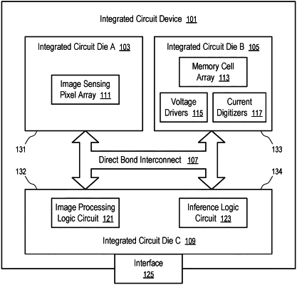
1. A device, comprising:
a memory cell array, wherein each respective memory cell in the memory cell array has a threshold voltage programmable in a first mode to perform operations of multiplication and accumulation; and
a logic circuit;
wherein the memory cell array has a plurality of regions operable in parallel to perform operations of multiplication and accumulation, the plurality of regions including a first region and a second region;
wherein the logic circuit is configured to adjust, when at least a second portion of weight bits stored in the second region is an inverted version of a first portion of weight bits stored in the first region, a computation result of multiplication and accumulation generated using the second region to account for weight inversion and generate an output result based on a plurality of results generated using the plurality of regions respectively.
|