| CPC G11C 16/3431 (2013.01) [G06F 17/16 (2013.01); G06N 3/063 (2013.01); G11C 11/5628 (2013.01); G11C 11/5635 (2013.01); G11C 11/5642 (2013.01); G11C 16/0416 (2013.01); G11C 16/0466 (2013.01); G11C 16/0483 (2013.01); G11C 16/0491 (2013.01); G11C 16/10 (2013.01); H01L 29/0847 (2013.01); H01L 29/1037 (2013.01); H01L 29/40117 (2019.08); H01L 29/66833 (2013.01); H01L 29/78633 (2013.01); H01L 29/7926 (2013.01); H01L 29/92 (2013.01); H10B 43/27 (2023.02); H10B 43/10 (2023.02)] | 19 Claims |

|
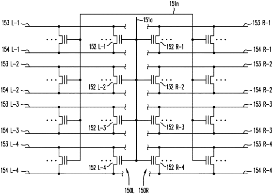
1. A 3-dimensional array of NOR memory strings formed above a planar surface of a semiconductor substrate, wherein each NOR memory string comprises:
a first group of thin-film memory transistors; and
a second group of thin-film memory transistors, wherein the thin-film memory transistors in the first group and the thin-film memory transistors in the second group share a common drain region and a common source region, wherein the thin-film memory transistors in the first group are configured to be accessed within a first access time and the thin-film memory transistors in the second group are configured to be accessed within a second access time, and wherein the first access time is less than the second access time.
|