| CPC G11C 16/30 (2013.01) [H02M 3/07 (2013.01); G11C 5/145 (2013.01); G11C 16/0483 (2013.01); G11C 16/32 (2013.01)] | 14 Claims |
|
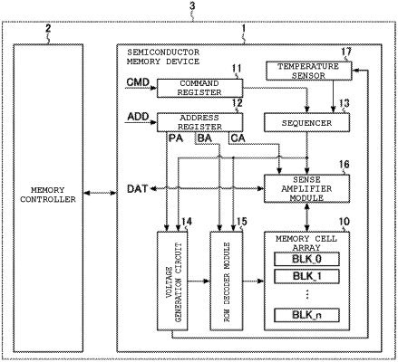
1. A voltage generation circuit comprising:
a plurality of charge pumps each connected to a first node;
a control circuit configured to control a number of active charge pumps among the plurality of charge pumps based on a period in which a voltage of the first node satisfies a predetermined condition; and
wherein the control circuit is configured to reduce the number of active charge pumps based on a first period in which the voltage of the first node is at least a first voltage in a state where at least two charge pumps among the plurality of charge pumps are active.
|