| CPC G11C 16/24 (2013.01) [G06F 13/1668 (2013.01); G11C 11/5628 (2013.01); G11C 16/0483 (2013.01); G11C 16/08 (2013.01); G11C 16/10 (2013.01); G11C 16/26 (2013.01); G11C 16/3418 (2013.01); G06F 2213/0024 (2013.01); G11C 16/14 (2013.01); G11C 2211/5648 (2013.01); H10B 41/27 (2023.02); H10B 41/35 (2023.02); H10B 43/27 (2023.02); H10B 43/35 (2023.02)] | 20 Claims |

|
1. A memory device comprising:
a plurality of three-dimensional structures including a first structure and a second structure, each of the plurality of three-dimensional structures including:
a plurality of NAND strings that include a first NAND string and a second NAND string, each of the plurality of NAND strings including:
a plurality of memory cells that include a plurality of first memory cells and a plurality of second memory cells, and
a plurality of sub-blocks that include a first sub-block and a second sub-block;
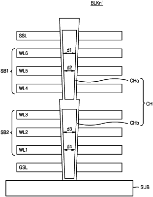
a first channel disposed in the first sub-block;
a second channel disposed in the second sub-block; and
a control logic configured to program the plurality of first memory cells on the first NAND string in a first sub-block of the first structure in a first order, and to program the plurality of second memory cells on the second NAND string in a second sub-block of the second structure in a second order that is different from the first order, wherein:
the plurality of first memory cells of each of the plurality of NAND strings are disposed in the first sub-block of each of the plurality of three-dimensional structures,
the first sub-block of the first structure is disposed at the same vertical level as a first sub-block of the second structure,
a horizontal width of an upper portion of the first channel is greater than a horizontal width of a lower portion of the first channel,
a horizontal width of an upper portion of the second channel is greater than a horizontal width of a lower portion of the second channel,
the first channel and the second channel are connected to each other and configured to form one channel of each of the plurality of NAND strings,
the upper portion of the second channel is connected to the lower portion of the first channel at a particular vertical level, and
at the particular vertical level, the horizontal width of the upper portion of the second channel is greater than the horizontal width of the lower portion of the first channel.
|