| CPC G11C 16/16 (2013.01) [G06F 3/0604 (2013.01); G06F 3/064 (2013.01); G06F 3/0652 (2013.01); G06F 3/0679 (2013.01); G11C 11/5628 (2013.01); G11C 11/5635 (2013.01); G11C 11/5642 (2013.01); G11C 11/5671 (2013.01); G11C 16/0483 (2013.01); G11C 16/10 (2013.01); G11C 16/26 (2013.01); G11C 16/3445 (2013.01); H10B 41/27 (2023.02); H10B 43/27 (2023.02)] | 15 Claims |

|
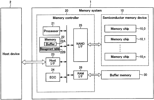
1. A memory system comprising:
a semiconductor memory device including a plurality of memory cells, each of the plurality of memory cells being configured to store n-bit data corresponding to a first threshold voltage range to a 2 n-th threshold voltage range, n being an integer of 2 or more, an (m+1)-th threshold voltage range being greater than an m-th threshold voltage range, m being a natural number and m being (2 n−1) or less; and
a memory controller configured to send a parameter and a command to the semiconductor memory device, the parameter relating to an erase voltage for an erase operation with respect to the plurality of memory cells, the command instructing the erase operation, wherein
the plurality of memory cells includes a first plurality of memory cells
the semiconductor memory device includes a first word line connected to the first plurality of memory cells,
the semiconductor memory device is configured to execute, based on the parameter, the erase operation for erasing the n-bit data in the plurality of memory cells in response to the command,
the memory controller is configured to send a read command to the semiconductor memory device after the semiconductor memory device executes the erase operation,
the semiconductor memory device is configured to read data from the first plurality of memory cells by applying a first voltage to the first word line in response to the read command, the first voltage being lower than a voltage between the first threshold voltage range and a second threshold voltage range, the second threshold voltage range being a threshold voltage range among the first threshold voltage range to the 2 n-th threshold voltage range, excluding the first threshold voltage range,
the semiconductor memory device is configured to send the read data as a first data to the memory controller, and
the memory controller is configured to update the parameter based on the first data which the semiconductor memory device sends in response to the read command.
|