| CPC G11C 16/10 (2013.01) [G11C 16/0483 (2013.01); G11C 16/3459 (2013.01)] | 9 Claims |

|
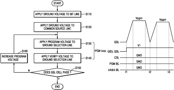
1. A program method, comprising:
applying a first voltage to a plurality of bit lines;
applying a second voltage to a common source line (CSL);
performing a program loop by applying a program voltage and a verify voltage to each of a plurality of ground selection lines (GSLs) positioned between one bit line among the plurality of bit lines and the CSL,
wherein the program loop is performed on both a program completed cell in which a program is completed by applying the program voltage and a program target cell;
determining whether GSL cells respectively connected to the GSLs pass; and
increasing the program voltage when there is at least one fail cell among the GSL cells, and repeatedly performing the program loop on the plurality of GSLs based on the increased program voltage by applying the first voltage to an inhibit bit line connected to a pass cell among the GSL cells and to a program bit line connected to at least one fail cell among the GSL cells without distinguishing between the inhibit bit line and the program bit line.
|