| CPC G11C 11/4099 (2013.01) [G11C 11/4074 (2013.01); G11C 11/4085 (2013.01)] | 9 Claims |

|
1. A nonvolatile memory device, comprising:
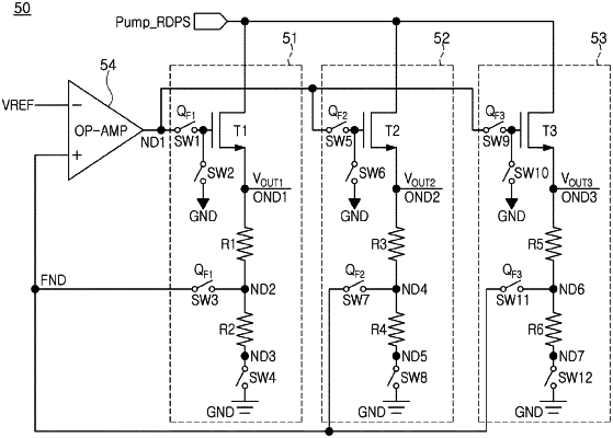
an operational amplifier configured to compare a reference voltage with a voltage of a feedback node;
a first feedback network circuit configured to generate a first output voltage by dividing an input voltage in response to an output voltage of the operational amplifier, to apply the first output voltage to a first set of wordlines, and to transmit a first feedback voltage corresponding to the first output voltage to the feedback node in response to a first feedback signal;
a second feedback network circuit configured to generate a second output voltage by dividing the input voltage in response to the output voltage of the operational amplifier, to apply the second output voltage to a second set of wordlines, and to transmit a second feedback voltage corresponding to the second output voltage to the feedback node in response to a second feedback signal; and
a third feedback network circuit configured to generate a third output voltage by dividing the input voltage in response to the output voltage of the operational amplifier, to apply the third output voltage to a third set of wordlines, and to transmit a third feedback voltage corresponding to the third output voltage to the feedback node in response to a third feedback signal,
wherein each of the first to third feedback network circuits include two resistors connected in series and a switch, and divides the input voltage by two resistors,
wherein one end of the switch is connected between the two resistors connected in series, and the other end of the switch is connected to the feedback node.
|