| CPC G11C 11/4085 (2013.01) [G11C 5/063 (2013.01); G11C 11/4074 (2013.01); G11C 11/4087 (2013.01); G11C 11/4094 (2013.01)] | 20 Claims |

|
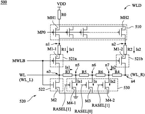
1. A memory device, comprising:
a first driving circuit configured to provide a first current signal from a first node to a second node according to a decoder signal;
a second driving circuit configured to provide a second current signal from the first node to a third node according to the decoder signal;
a third driving circuit configured to couple the first node to a reference voltage terminal according to the decoder signal;
a first switch configured to transmit the first current signal to the reference voltage terminal;
a second switch separated from the first switch, and configured to transmit the second current signal to the reference voltage terminal; and
a modulating circuit configured to transmit each of the first current signal and the second current signal to the reference voltage terminal when the first switch and the second switch are turned off.
|