| CPC G09G 3/3674 (2013.01) [G09G 3/20 (2013.01); G09G 3/3688 (2013.01); G11C 19/28 (2013.01); H03K 3/356026 (2013.01); H03K 5/15066 (2013.01); H03K 5/15093 (2013.01); G09G 2310/0267 (2013.01); G09G 2310/0283 (2013.01); G09G 2310/0286 (2013.01); G11C 19/287 (2013.01); H03K 4/026 (2013.01)] | 1 Claim |

|
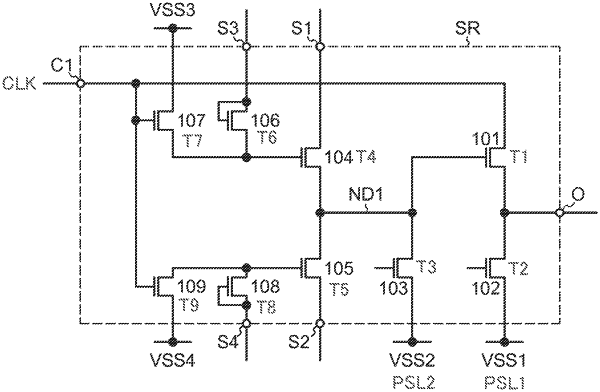
1. A semiconductor device comprising:
a first transistor, a second transistor, a third transistor, a fourth transistor, a fifth transistor, a sixth transistor, a seventh transistor, an eighth transistor and a ninth transistor,
wherein one of a source and a drain of the first transistor is electrically connected to a clock signal line,
wherein the other of the source and the drain of the first transistor is electrically connected to an output terminal,
wherein one of a source and a drain of the second transistor is electrically connected to the output terminal,
wherein the other of the source and the drain of the second transistor is electrically connected to a first power supply line,
wherein one of a source and a drain of the third transistor is electrically connected to a gate of the first transistor,
wherein the other of the source and the drain of the third transistor is electrically connected to a second power supply line,
wherein one of a source and a drain of the fourth transistor is electrically connected to the gate of the first transistor,
wherein one of a source and a drain of the fifth transistor is electrically connected to the gate of the first transistor,
wherein one of a source and a drain of the sixth transistor is electrically connected to a gate of the fourth transistor,
wherein the other of the source and the drain of the sixth transistor is electrically connected to a first signal line,
wherein a gate of the sixth transistor is electrically connected to the other of the source and the drain of the sixth transistor,
wherein one of a source and a drain of the seventh transistor is electrically connected to the gate of the fourth transistor,
wherein one of a source and a drain of the eighth transistor is electrically connected to a gate of the fifth transistor,
wherein the other of the source and the drain of the eighth transistor is electrically connected to a second signal line,
wherein a gate of the eighth transistor is electrically connected to the other of the source and the drain of the eighth transistor,
wherein one of a source and a drain of the ninth transistor is electrically connected to the gate of the fifth transistor,
wherein a gate of the ninth transistor is electrically connected to a gate of the seventh transistor,
wherein the fourth transistor is configured to control a potential of the gate of the first transistor,
wherein the fifth transistor is configured to control a potential of the gate of the first transistor,
wherein the seventh transistor is configured to control a potential of the gate of the fourth transistor, and
wherein the ninth transistor is configured to control a potential of the gate of the fifth transistor.
|