| CPC G09G 3/3291 (2013.01) [G09G 3/3225 (2013.01); G09G 3/3233 (2013.01); G09G 3/3266 (2013.01); G09G 2300/0842 (2013.01); G09G 2310/027 (2013.01); G09G 2310/0278 (2013.01); G09G 2310/08 (2013.01); G09G 2320/0233 (2013.01)] | 10 Claims |
|
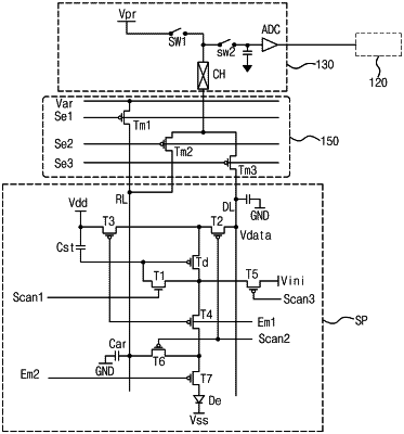
1. An organic light emitting diode display device, comprising:
a timing controlling circuit for generating an image data, a data control signal and a gate control signal;
a data driving circuit for generating a data voltage based on the image data and the data control signal, the data driving circuit including an output channel for outputting the data voltage and a pre-charge voltage in two different operations, respectively;
a gate driving circuit for generating a first gate voltage, a second gate voltage, a third gate voltage, a first emission voltage and a second emission voltage based on the gate control signal;
a display panel including a subpixel, a gate line, a data line and a reset line, the subpixel including first, second, third, fourth, fifth, sixth, and seventh transistors, a storage capacitor and a light emitting diode, the gate line for transmitting the first gate voltage, the second gate voltage, the third gate voltage, the first emission voltage, and the second emission voltage to the subpixel, and the reset line for transmitting the pre-charge voltage to the subpixel; and
a selecting circuit connecting the output channel to one of the data line or the reset line, the selecting circuit including a first mux transistor a second mux transistor and a third mux transistor, the second mux transistor configured to connect the pre-charge voltage to an anode of the light emitting diode through the reset line in a first operation and connect the anode of the light emitting diode to a voltage detecting unit through the reset line in a second operation subsequent to the first operation, the third mux transistor configured to connect the data voltage to the data line in a third operation subsequent to the second operation, and the data line different from the reset line.
|