| CPC G09G 3/3275 (2013.01) [G09G 3/3266 (2013.01); G09G 2300/043 (2013.01); G09G 2310/0278 (2013.01); G09G 2310/0286 (2013.01); G09G 2310/08 (2013.01); G09G 2330/021 (2013.01)] | 13 Claims |

|
1. A display device using a display element driven by a current, the display device comprising:
a display portion including a plurality of data signal lines, a plurality of first scanning signal lines, a plurality of second scanning signal lines, a plurality of first light emission control lines, a plurality of second light emission control lines, a first power source line, a second power source line, an initialization power source line, and a plurality of pixel circuits;
a data-side drive circuit configured to apply data signals to the plurality of data signal lines; and
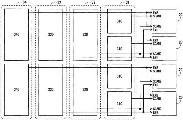
a scanning-side drive circuit including a first scanning signal line drive circuit configured to selectively drive the plurality of first scanning signal lines, a second scanning signal line drive circuit configured to selectively drive the plurality of second scanning signal lines, and a light emission control line drive circuit configured to selectively drive the plurality of first light emission control lines and the plurality of second light emission control lines,
wherein each of the plurality of pixel circuits corresponds to one of the plurality of data signal lines, one of the plurality of first scanning signal lines, one of the plurality of second scanning signal lines, one of the plurality of first light emission control lines, and one of the plurality of second light emission control lines,
each of the plurality of pixel circuits includes
the display element including a first terminal, and a second terminal connected to the second power source line,
a drive transistor including a control terminal, a first conduction terminal, and a second conduction terminal, and provided in series with the display element,
a holding capacitor connected at one end to the control terminal of the drive transistor,
a writing control transistor including a control terminal connected to a corresponding second scanning signal line, a first conduction terminal connected to a corresponding data signal line, and a second conduction terminal connected to the second conduction terminal of the drive transistor,
a threshold voltage compensation transistor including a control terminal connected to a corresponding first scanning signal line, a first conduction terminal connected to the first conduction terminal of the drive transistor, and a second conduction terminal connected to the control terminal of the drive transistor,
a power supply control transistor including a control terminal connected to a corresponding second light emission control line, a first conduction terminal connected to the first power source line, and a second conduction terminal connected to the first conduction terminal of the drive transistor,
a light emission control transistor including a control terminal connected to a corresponding first light emission control line, a first conduction terminal connected to the second conduction terminal of the drive transistor, and a second conduction terminal connected to the first terminal of the display element, and
an initialization transistor including a control terminal connected to a corresponding first scanning signal line, a first conduction terminal connected to the first terminal of the display element, and a second conduction terminal connected to the initialization power source line,
the first scanning signal line drive circuit is constituted by a shift register including unit circuits equal in number to a number of the plurality of first scanning signal lines,
the second scanning signal line drive circuit is constituted by a shift register including unit circuits equal in number to 1/Q of a number of the plurality of second scanning signal lines, where Q is an integer of 2 or greater,
each of the unit circuits included in the shift register constituting the first scanning signal line drive circuit drives one corresponding first scanning signal line,
each of the unit circuits included in the shift register constituting the second scanning signal line drive circuit collectively drives Q second scanning signal lines corresponding thereto and adjacent to each other, and
in a period during which the writing control transistor is maintained in an on state in all pixel circuits each being connected to any one of Q second scanning signal lines collectively driven in a period during which the power supply control transistor and the light emission control transistor are maintained in an off state in the all pixel circuits each being connected to any one of the Q second scanning signal lines collectively driven, Q first scanning signal lines corresponding to the Q second scanning signal lines collectively driven are sequentially set to a select state for a predetermined period each.
|