| CPC G09G 3/3266 (2013.01) [G09G 2300/0426 (2013.01); G09G 2310/0286 (2013.01); G09G 2310/08 (2013.01)] | 20 Claims |

|
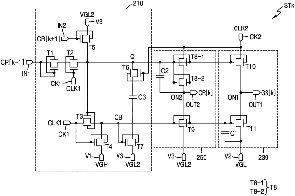
1. A gate driving circuit comprising:
a plurality of stages, each comprising:
a node controller that controls voltage levels of a first node and a second node;
a first output portion that outputs a gate signal having a voltage of a first level or a voltage of a second level lower than the first level according to the voltage levels of the first node and the second node;
a second output portion that outputs a carry output signal having the voltage of the first level or a voltage of a third level lower than the second level according to the voltage levels of the first node and the second node, wherein
the node controller comprises:
a first stabilization transistor and a second stabilization transistor electrically connected in series between the first node and a voltage input terminal to which the voltage of the third level is applied; and
a first capacitor electrically connected between the first stabilization transistor and the second stabilization transistor,
the first stabilization transistor is electrically connected between the first node and the first capacitor and including a gate electrically connected to a first clock input terminal to which a first clock signal is applied, and
the second stabilization transistor is electrically connected between the first capacitor and the voltage input terminal to which the voltage of the third level is applied and including a gate electrically connected to the second node.
|