| CPC G09G 3/3258 (2013.01) [G09G 3/3266 (2013.01); G09G 3/3275 (2013.01); G09G 2300/0871 (2013.01); G09G 2310/0202 (2013.01); G09G 2310/08 (2013.01); G09G 2320/0257 (2013.01); G09G 2330/02 (2013.01)] | 7 Claims |

|
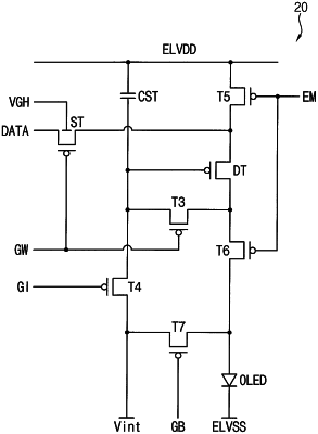
1. A display device, comprising:
a display panel including a plurality of pixel circuits; and
a panel driving part that provides a scan signal, a data voltage, a high power supply voltage, and a low power supply voltage to the display panel,
wherein each of the plurality of pixel circuits comprises:
an organic light emitting diode;
a switching transistor that is turned off when the scan signal has a first voltage and turned on when the scan signal has a second voltage, the switching transistor including a second bottom gate electrode that is provided with a constant voltage equal to the first voltage, wherein the constant voltage is larger than 0V or less than 0V;
a storage capacitor that stores the data voltage provided through a data line when the switching transistor is turned on;
a driving transistor that provides a driving current to the organic light emitting diode, the driving current corresponding to the data voltage stored in the storage capacitor, the driving transistor having a gate electrode directly connected to the storage capacitor and a first power electrode directly connected the switching transistor; and
a third transistor to compensate a threshold voltage for the driving transistor, the third transistor electrically connected between a second power electrode of the driving transistor and the gate electrode of the driving transistor,
the second bottom gate electrode is electrically disconnected from the driving transistor, and
wherein the panel driving part includes a gate driver that is provided with the first voltage and generates the scan signal.
|