| CPC G09G 3/3233 (2013.01) [G09G 2300/0819 (2013.01); G09G 2300/0852 (2013.01); G09G 2300/0861 (2013.01); G09G 2310/08 (2013.01); G09G 2320/0223 (2013.01); G09G 2320/0233 (2013.01)] | 18 Claims |

|
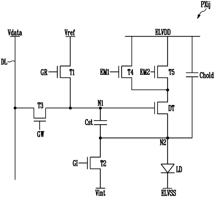
1. A pixel comprising:
a light emitting element;
a driving transistor having an electrode electrically connected to an anode electrode of the light emitting element and another electrode electrically connected to a first power source and controlling a current flowing from the first power source to a second power source through the light emitting element;
a first transistor electrically connected between a gate electrode of the driving transistor and a reference power source;
a second transistor electrically connected between the anode electrode of the light emitting element and an initialization power source;
a third transistor electrically connected between the gate electrode of the driving transistor and a data line; and
a fourth transistor and a fifth transistor electrically connected in parallel between the first power source and the another electrode of the driving transistor, wherein
the fourth transistor compensates a threshold voltage of the driving transistor by electrically connecting the another electrode of the driving transistor to the first power source during a compensation period, and
the fifth transistor is turned so that the current flowing through the light emitting element is controlled according to a control of the driving transistor during an emission period of the light emitting element.
|