| CPC G09G 3/3233 (2013.01) [H10K 59/1213 (2023.02); G09G 2300/0426 (2013.01); G09G 2300/0452 (2013.01); G09G 2300/0819 (2013.01); G09G 2300/0842 (2013.01); G09G 2320/0233 (2013.01); G09G 2330/021 (2013.01)] | 6 Claims |

|
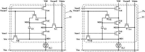
1. A display device comprising a first transistor, a second transistor, a third transistor, and a light-emitting element,
wherein the light-emitting element is electrically connected to one of a source and a drain of the first transistor,
wherein the other of the source and the drain of the first transistor is electrically connected to one of a source and a drain of the second transistor,
wherein a gate electrode of the second transistor is electrically connected to one of a source and a drain of the third transistor,
wherein a semiconductor layer of the second transistor comprises indium, zinc, and an element M,
wherein the element M is one or more kinds selected from gallium, aluminum, yttrium, tin, silicon, boron, copper, vanadium, beryllium, titanium, iron, nickel, germanium, zirconium, molybdenum, lanthanum, cerium, neodymium, hafnium, tantalum, tungsten, magnesium, and cobalt,
wherein a semiconductor layer of the third transistor comprises indium, zinc and the element M,
wherein a ratio of the number of indium atoms to a total number of the indium atoms, zinc atoms, and atoms of the element M in the semiconductor layer of the second transistor is higher than or equal to 30 atomic % and lower than or equal to 100 atomic %,
wherein a ratio of the number of atoms of the element M to a total number of indium atoms, zinc atoms, and the atoms of the element M in the semiconductor layer of the third transistor is higher than that in the semiconductor layer of the second transistor, and
wherein the second transistor is configured to control the amount of light emission of the light-emitting element.
|