| CPC G09G 3/3233 (2013.01) [G09G 3/32 (2013.01); G09G 2300/0842 (2013.01); G09G 2310/061 (2013.01); G09G 2330/021 (2013.01)] | 19 Claims |

|
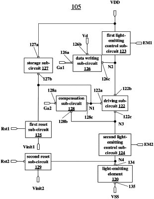
1. A display substrate, comprising:
a base substrate, comprising a display region, wherein the display region comprises a plurality of sub-pixels arranged in array, each of the plurality of sub-pixels comprises a pixel driving circuit and a light-emitting element, and the pixel driving circuit is configured to drive the light-emitting element to emit light; and
a plurality of reset signal lines extending in a first direction, wherein the plurality of reset signal lines comprise a plurality of first reset signal lines for providing a first reset signal and a plurality of second reset signal lines for providing a second reset signal, and one of the plurality of first reset signal lines and one of the plurality of second reset signal lines are respectively connected to pixel driving circuits of a plurality of sub-pixels located in a same row, wherein
a layer where the plurality of first reset signal lines are located is different from layers where the plurality of second reset signal lines are located,
the plurality of sub-pixels are arranged in N rows;
one of the plurality of second reset signal lines is electrically connected to pixel driving circuits of sub-pixels in an (M−1)th row, and one of the plurality of first reset signal lines is electrically connected to pixel driving circuits of sub-pixels in an (M)th row; and
an orthographic projection of a second reset signal line, that is electrically connected to the pixel driving circuits of the sub-pixels in the (M−1)th row, on the base substrate at least partially overlaps with an orthographic projection of a first reset signal line, that is electrically connected to the pixel driving circuits of the sub-pixels in the (M)th row, on the base substrate, wherein 1<M≤N, and M and N are positive integers greater than or equal to 2.
|