| CPC G09G 3/3233 (2013.01) [G09G 2300/0426 (2013.01); G09G 2310/061 (2013.01)] | 17 Claims |

|
1. An array substrate, comprising:
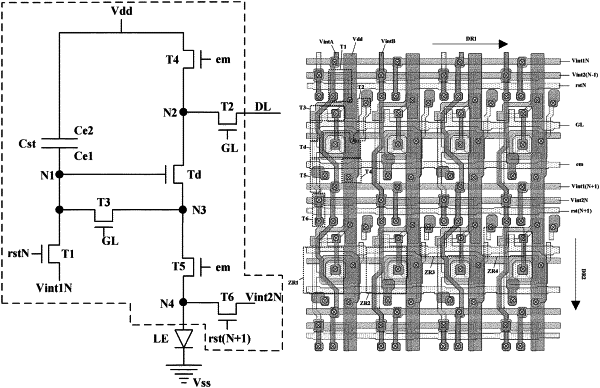
K number of reset signal lines respectively configured to provide reset signals to reset transistors in K columns pixel driving circuits of the array substrate;
wherein the K number of reset signal lines comprises:
a plurality of third reset signal lines in (2k−1)-th columns of K columns, K and k being positive integers, 1≤ k≤ (K/2); and
a plurality of fourth reset signal lines in (2k)-th columns of the K columns;
wherein the array substrate comprises a first interconnected reset signal supply network and a second interconnected reset signal supply network;
wherein the first interconnected reset signal supply network comprises the plurality of third reset signal lines in the (2k−1)-th columns, and a plurality of first reset signal lines respectively cross over the plurality of third reset signal lines; and
the second interconnected reset signal supply network comprises the plurality of fourth reset signal lines in the (2k)-th columns, and a plurality of second reset signal lines respectively cross over the plurality of fourth reset signal lines;
wherein the array substrate further comprises a first initialization connecting line present in a (2k)-th column, and absent in a (2k−1)-th column and a second initialization connecting line present in the (2k−1)-th column, and absent in the (2k)-th column;
wherein the first initialization connecting line in the (2k)-th column connects a respective first reset signal line of the plurality of first reset signal lines and a source electrode of a first reset transistor in a respective pixel driving circuit in the (2k)-th column together;
the second initialization connecting line in the (2k−1)-th column connects a respective second reset signal line of the plurality of second reset signal lines and a source electrode of a second reset transistor in a respective pixel driving circuit in the (2k−1)-th column together;
a respective third reset signal line in the (2k−1)-th column connects a respective first reset signal line of the plurality of first reset signal lines and a source electrode of a first reset transistor in the respective pixel driving circuit in the (2k−1)-th column together; and
a respective fourth reset signal line in the (2k)-th column connects a respective second reset signal line of the plurality of second reset signal lines and a source electrode of a second reset transistor in the respective pixel driving circuit in the (2k)-th column together.
|