| CPC G09G 3/32 (2013.01) [B60K 35/00 (2013.01); G09G 5/10 (2013.01); B60K 35/22 (2024.01); B60K 2360/1523 (2024.01); B60K 2360/349 (2024.01); G09G 2320/0633 (2013.01)] | 9 Claims |

|
1. A display arrangement comprising:
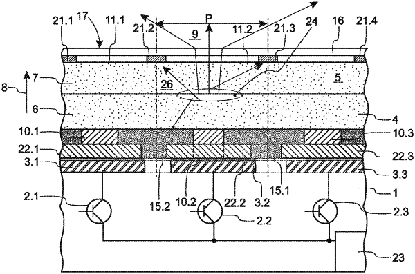
an IC substrate component with monolithic integrated circuits and with IC substrate contacts arranged as a matrix; a monolithic pixelated optochip comprising a semiconductor layer sequence with a first semiconductor layer having a first doping and a second semiconductor layer having a second doping, wherein the polarity of the charge carriers in the first semiconductor layer differs from that of the second semiconductor layer and the semiconductor layer sequence defines a stacking direction;
wherein μ-LEDs arranged as a matrix are present in the monolithic pixelated optochip;
wherein each μ-LED has a μ-LED rear side facing the IC substrate component and a first light source contact which adjoins the first semiconductor layer in a contacting manner and is electrically conductively connected to a respective one of the IC substrate contacts;
wherein the projection area of the first light source contact on the μ-LED rear surface is at most half the area of the μ-LED rear surface;
wherein the first light source contact in a lateral direction perpendicular to the stacking direction is surrounded by an absorber on the rear side;
wherein at least one of the first semiconductor layer or the second semiconductor layer is continuous across the μ-LEDs; and
wherein a second light source contact is adjacent to a transparent contact layer and the second light source contact of adjacent μ-LEDs are separated from each other by a front absorber on the front side in a lateral direction perpendicular to the stacking direction.
|