| CPC G09G 3/2096 (2013.01) [G09G 2310/0291 (2013.01); G09G 2330/04 (2013.01)] | 20 Claims |
|
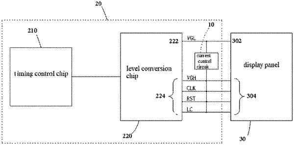
1. A current control circuit applied to a display panel driving device, comprising: a level conversion chip, the level conversion chip has a plurality of signal outputs, a plurality of signal outputs of the level conversion chip are configured to be connected to a plurality of signal inputs of the display panel in a one-to-one correspondence manner; a high level signal is output through a first signal output in a plurality of signal outputs of the level conversion chip when the level conversion chip receives a power-off instruction;
wherein the current control circuit comprises an energy storage unit, a first switch unit, and a pulse width modulation unit;
a first end of the energy storage unit is configured to be connected to the first signal output of the level conversion chip to receive the high level signal, a second end of the energy storage unit is configured to be connected to at least one second signal output of the level conversion chip, and the second signal output is other signal output(s) other than the first signal output in a plurality of signal outputs of the level conversion chip;
a first end of the first switch unit is configured to be connected to a first preset voltage terminal, a second end of the first switch unit is connected to a first end of the energy storage unit, and a control end of the first switch unit is connected to an output of the pulse width modulation unit; and
an output of the pulse width modulation unit is configured to output a pulse width modulation signal used for controlling a duty cycle of the first switch unit, and thereby controlling a magnitude of a voltage at a first end of the energy storage unit and a magnitude of a current in the energy storage unit.
|