| CPC G09G 3/2092 (2013.01) [G09G 2310/0267 (2013.01); G09G 2310/08 (2013.01)] | 18 Claims |

|
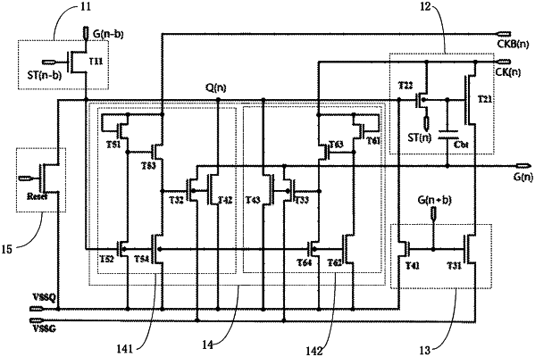
1. A gate driver on array GOA circuit, comprising a plurality of GOA units, which is cascaded, and a nth stage GOA unit comprises:
a pull-up control module, outputting a pull-up control signal of a high potential according to a n−bth stage transfer signal and a n−bth stage gate drive signal when scanning starts;
an output module, outputting a nth stage gate drive signal of the high potential according to the pull-up control signal of the high potential and a nth stage non-inverting clock signal;
a pull-down module, pulling down the pull-up control signal outputted by the pull-up control module and the nth stage gate drive signal outputted by the output module to a low potential according to a n+bth stage gate drive signal when the scanning is completed; and
a pull-down maintaining module, maintaining the pull-up control signal outputted by the pull-up control module and the nth stage gate drive signal outputted by the output module at the low potential according to the nth stage non-inverting clock signal and a nth stage inverting clock signal, wherein the nth stage non-inverting clock signal and the nth stage inverting clock signal are mutually inverted signals.
|