| CPC G06T 7/001 (2013.01) [G06T 5/50 (2013.01); G06V 10/761 (2022.01); G06T 2207/20221 (2013.01); G06T 2207/20224 (2013.01); G06T 2207/30148 (2013.01)] | 30 Claims |

|
1. A system configured to detect defects on a reticle, comprising:
an inspection subsystem configured to generate images for a wafer, wherein a reticle is used to print patterned areas on the wafer in a lithography process, and wherein the patterned areas comprise first patterned areas corresponding to the same area on the reticle and printed in different rows on the wafer; and
a computer subsystem configured for:
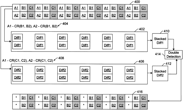
generating different stacked difference images for multiple instances of the first patterned areas in the different rows based on the images generated for the first patterned areas in the different rows by the inspection subsystem;
detecting defect candidates in the multiple instances of the first patterned areas on the wafer by applying a defect detection method to the different stacked difference images, wherein the defect detection method determines that a defect candidate is present at a location in each of the multiple instances of the first patterned areas only when the defect detection method detects the defect candidate at the location in the different stacked difference images; and
identifying defects on the reticle based on the detected defect candidates.
|