| CPC G06F 9/4405 (2013.01) [G06F 21/64 (2013.01)] | 20 Claims |

|
1. A processing system, comprising:
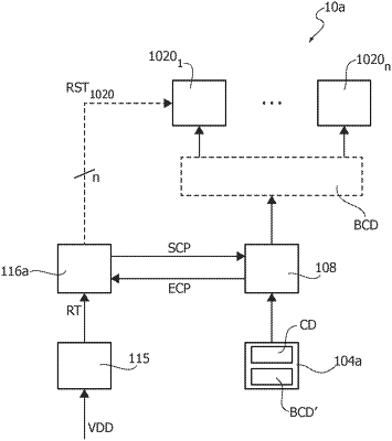
a power supply monitoring circuit configured to generate a reset request signal in response to the processing system being turned ON;
a plurality of microprocessors, each configured to start execution of instructions in accordance with a start address;
a reset management circuit configured to receive the reset request signal and, in response, sequentially execute a reset phase, a configuration phase, and a software runtime phase, wherein the processing system is configured to start execution of instructions by a microprocessor as a function of boot configuration data;
a register configured to store a first boot configuration data, the first boot configuration data including a boot record indicating which one of the microprocessors is to be started and a respective start address;
a plurality of configuration data client circuits configured to store configuration data, each configuration data client circuit having an address data, each configuration data client circuit configured to receive a write request and configured to store data included in the write request to a register of the configuration data client circuit in response to the write request having an address data corresponding to the address data associated with the configuration data client circuit, wherein a configuration data client circuit is configured to provide a second boot configuration data indicating a start address and whether the processing system is to use a default boot configuration or a user-defined boot configuration;
a non-volatile memory configured to store the first boot configuration data at predetermined memory locations, the first boot configuration data being stored in the form of data records, each data record of the first boot configuration data having an associated address of a configuration data client circuit and an associated data to be stored at the configuration data client circuit; and
a hardware configuration circuit configured to:
read the boot record from the predetermined memory locations,
store the boot record to the register,
sequentially read the data records of the first boot configuration data from the non-volatile memory, and
generate a respective write request for each data record, the write request being used to store data of the data record to the configuration data client circuit with the address data indicated in the data record,
wherein the hardware configuration circuit and the reset management circuit are configured to:
start a predetermined microprocessor at a default start address in response to determining that the second boot configuration data indicates that the processing system is to use the default boot configuration,
start a microprocessor at the start address as indicated by the boot record stored to the register in response to determining that the second boot configuration data indicates that the processing system is to use the user-defined boot configuration and the registers have stored a valid boot record, and
start the predetermined microprocessor at the start address indicated by the second boot configuration data in response to the determining that the second boot configuration data indicates that the processing system is to use the user-defined boot configuration and the registers do not have a valid boot record.
|