| CPC G06F 30/327 (2020.01) [G06F 2111/06 (2020.01); G06F 2119/18 (2020.01)] | 20 Claims |
|
1. A logic circuit for providing a multibit flip-flop (MBFF) function, the logic circuit comprising:
a first inverter configured to receive a clock signal and generate a corresponding clock_bar signal;
a second inverter configured to receive the clock_bar signal and generate a corresponding clock_bar_bar signal;
a third inverter configured to receive a control signal and generate a corresponding control_bar signal; and
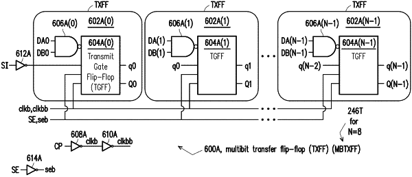
a series-chain of 1-bit transfer flip-flop (TXFF) circuits, each TXFF circuit including:
a NAND circuit configured to receive data signals; and
a 1-bit transmit gate flip-flop (TGFF) circuit configured to:
output signals Q and q; and
receive an output of the NAND circuit, the signal q from the TGFF circuit of a preceding TXFF circuit in the series-chain, the clock_bar signal, the clock_bar_bar signal, the control signal and the control_bar signal; and
a first one of the TXFF circuits in the series-chain being configured to receive a start signal in place of the signal q from an otherwise preceding TGFF circuit.
|